
Product Details:
Payment & Shipping Terms:
|
| Wave Length: | 355um | Super: | Low Power Consumption |
|---|---|---|---|
| Laser: | 12/15/17W | Laser Brand: | Optowave |
| Power: | 220V 380v | Warranty: | 1 Year |
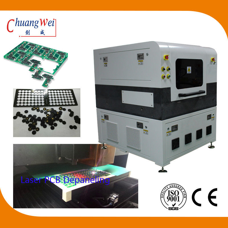
| Name: | Laser PCB Separator | ||
| Highlight: | medical Drying Cabinet,desiccant dry cabinets |
||
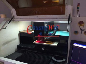
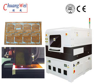
10W UV Optowave Laser PCB Separator Machine for Non Contact Depaneling
PCB depaneling (singulation) laser machines and systems have been gaining popularity over recent years. Mechanical depanaling/singulation is done with routing, die cutting, and dicing saw methods. However, as the boards get smaller, thinner, flexible, and more sophisticated, those methods produce even more exaggerated mechanical stress to the parts. Large boards with heavy substrates absorb these stresses better, while these methods used on ever-shrinking and complex boards can result in breakage. This brings lower throughput, along with the added costs of tooling and waste removal associated with mechanical methods.
Increasingly, flexible circuits are found in the PCB industry, and they also present challenges to the old methods. Delicate systems reside on these boards and non-laser methods struggle to cut them without damaging the sensitive circuitry. A non-contact depaneling method is required and lasers provide a highly precise way of singulation without any risk of harming them, regardless of substrate.
Challenges of Depaneling using Routing/Die Cutting/Dicing Saws
Lasers, on the other hand, are gaining control of the PCB depaneling/singulation market due to higher precision, lower stress on the parts, and higher throughput. Laser depaneling can be applied to a variety of applications with a simple change in settings. There is no bit or blade sharpening, lead time reordering dies and parts, or cracked/broken edges due to torque on the substrate. Application of lasers in PCB depaneling is dynamic and a non-contact process.
Advantages of Laser PCB Depaneling/Singulation
Laser PCB Depaneling Specification
| Laser class | 1 |
| Max. working area (X x Y x Z) | 300 mm x 300 mm x 11 mm |
| Max. recognition area (X x Y) | 300 mm x 300 mm |
| Max. material size (X x Y) | 350 mm x 350 mm |
| Data input formats | Gerber, X-Gerber, DXF, HPGL, |
| Max. structuring speed | Depends on application |
| Positioning accuracy | ± 25 μm (1 Mil) |
| Diameter of focused laser beam | 20 μm (0.8 Mil) |
| Laser wavelength | 355 nm |
| System dimensions (W x H x D) | 1000mm*940mm *1520 mm |
| Weight | ~ 450 kg (990 lbs) |
| Operating conditions | |
| Power supply | 230 VAC, 50-60 Hz, 3 kVA |
| Cooling | Air-cooled (internal water-air cooling) |
| Ambient temperature | 22 °C ± 2 °C @ ± 25 μm / 22 °C ± 6 °C @ ± 50 μm (71.6 °F ± 3.6 °F @ 1 Mil / 71.6 °F ± 10.8 °F @ 2 Mil) |
| Humidity | < 60 % (non-condensing) |
| Required accessoires | Exhaust unit |
More information welcome to contact us:
Email/Skype: s5@smtfly.com
Mobile/Wechat/WhatsApp: +86-136-8490-4990
Contact Person: Mr. Alan
Tel: 86-13922521978
Fax: 86-769-82784046